
We have compiled a list of manufacturers, distributors, product information, reference prices, and rankings for Gallium Nitride Wafer.
ipros is IPROS GMS ・ IPROS One of the largest technical database sites in Japan that collects information on.

Gallium Nitride Wafer - List of Manufacturers, Suppliers, Companies and Products | IPROS GMS

Gallium Nitride Wafer Product List

1~2 item / All 2 items

Displayed results

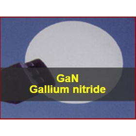
GaN (Gallium Nitride)

It is also expected to be a next-generation power semiconductor device.

This is an introduction to "GaN (Gallium Nitride)," the main product of Shinyo Corporation. Compared to silicon, it has a bandgap that is about three times wider (3.42 eV) and an insulation breakdown voltage that is about ten times higher (3.0 MV/cm). When the on-resistance is reduced to the same level as silicon at 10 mΩ·cm², the withstand voltage reaches 1600 V. Additionally, it can generate relatively short wavelengths of light, such as blue and green, and is used in various optical devices, making it a promising candidate for next-generation power semiconductor devices alongside SiC. 【Features】 ■ Bandgap is about three times wider compared to silicon ■ Insulation breakdown voltage is about ten times higher ■ Withstand voltage of 1600 V ■ Capable of generating relatively short wavelengths of light, such as blue and green ■ Used in various optical devices *For more details, please refer to the PDF materials or feel free to contact us.

  • Other polymer materials
  • Gallium Nitride Wafer

Added to bookmarks

Bookmarks list

Bookmark has been removed

Bookmarks list

You can't add any more bookmarks

By registering as a member, you can increase the number of bookmarks you can save and organize them with labels.

Free membership registration

Gallium nitride (GaN), SiC (silicon carbide) wafers

We offer 6-inch SiC substrate wafers, 6-inch GaN-on-Si HEMT RF epitaxial wafers, and more.

Best-selling products: 6-inch GaN-on-Si HEMT RF epitaxial wafers, 6-inch GaN-on-Si HEMT D-mode power epitaxial wafers, 6-inch GaN-on-Si HEMT E-mode power epitaxial wafers, 6-inch SiC substrate wafers, SiC substrate wafers (n-type substrate with a diameter of 150mm), etc. Suitable for research and development experimental supplies. Excellent cost performance.

  • Wafer
  • Other laboratory equipment and containers
  • Gallium Nitride Wafer

Added to bookmarks

Bookmarks list

Bookmark has been removed

Bookmarks list

You can't add any more bookmarks

By registering as a member, you can increase the number of bookmarks you can save and organize them with labels.

Free membership registration